
flowers of fire and light by Audrey C. '24
making art with printed circuit boards!
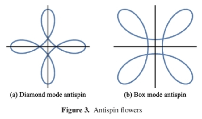
My favorite poi spinning pattern is the four-petaled antispin flower. If you do it neatly, it traces out the path parameterized by these equations:
x = cos(t) + 3/4 cos(-3t)
y = sin(t) + 3/4 sin(-3t)
From “Parametric Equations at the Circus: Trochoids and Poi Flowers” by Eleanor Farrington
The oblong “petals” are created by spinning the poi head in the opposite direction to that of the circle traced out by your arm, hence the term “antispin.” In other words, if your arm is moving clockwise, your wrist would be rotating counterclockwise. By modifying the number of petals, direction, timing, plane of movement, geometry, and other parameters, variations on the basic flower pattern encompasses a whole family of poi tricks. It’s fun to nerd out about the mathematical intricacies of poi spinning, but that’s a whole another topic that deserves its own blog.


I love the way the flower imagery bridges rigid geometry with the living and organic, inspiring me to recreate this pattern as LEDs on a printed circuit board (PCB). This would be a relatively straightforward project that would allow me to make all the mistakes that a beginner PCB designer would and to learn how to fix them.
Laying out the PCB
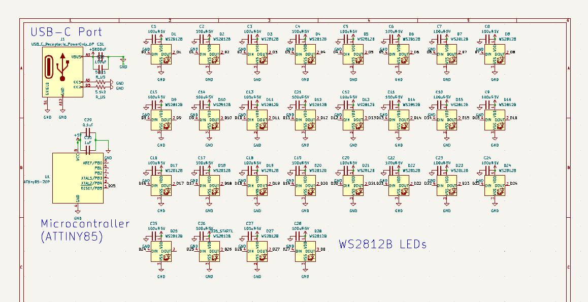
Having learned how to use Kicad from 2.67901 Electronics for Mechanical Systems II last semester, I use it here to design the PCB. The first step is to lay out all of the components in a schematic. My main components include a USB-C port to supply power, an ATtiny microcontroller to control the LEDs, and of course a bunch of LEDs. For this project, Kicad’s built in library already included all of the symbols for the components that I’m using.
Here we also specify how each component is connected to each other. Pins labeled with the same name indicate that they will be connected by a trace (copper wiring) later on.
The symbols on the schematic can represent a family of similar components, but how these components attach to the board can vary across manufacturers and variations of the same part. For example, through hole resistors and surface mount resistors can have the same resistance and therefore serve the same purpose. The former would require two holes, whereas the latter would require two solid copper pads.
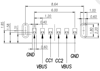
The exact pattern of the exposed copper on the board is called a footprint, which needs to be specified for each component. I’m hoping that Kicad would already have all the footprints for the components that I was planning to use, but alas no. I can’t find a suitable footprint for my USB-C port anywhere on the Internet, so I figure out how to make my own by referencing the part’s datasheet:

Once the footprints are specified, Kicad can “translate” the schematic into a board layout. The actual shape of the board, the location of the components, and how the traces are routed remain an exercise to the reader (or in this case, the maker?). Properly labeled schematics mean that at this step, Kicad only lets you connect two pins with a trace if you’re supposed to.
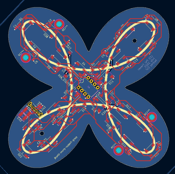
the board is supposed to resemble the diamond mode flower, but here it resembles the box mode flower because rotating the board actually makes it cheaper to fabricate
Ideally, your traces should be routed “correctly” at this point of the process, BEFORE you send it to the PCB manufacturer. Double check that everything is connected to what it’s supposed to. Triple check it.
Or not, and suffer later. :’)
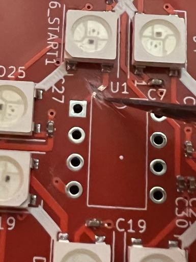
Rerouting traces on the physical board
Three weeks after I place my PCB order, I finally receive it in the mail! Because I want to get these boards completed as quickly as possible to give them out as gifts, I’ve opted for the manufacturer to solder many of the components for me. Five copies of my board, getting some of the components soldered, and shipping total to about $40.
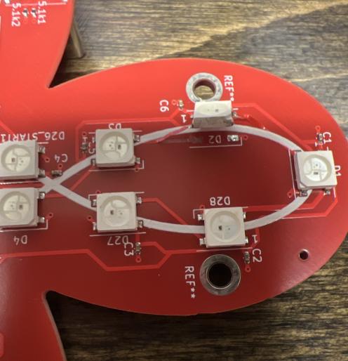
The joy of finally holding my physical boards turn into horror when I realize that I connected the LEDs to the RESET pin of the microcontroller. I could have chosen literally any other pin (except for ground and power, which are more obvious to avoid), and it wouldn’t have been a problem.
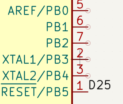
noooooo (D25 is the label that corresponds to the input of the first LED)
Luckily, Winnie, the amazing LA02 lab assistant who reviewed everyone’s PCBs in 2.679, reassures me that it won’t be necessary to pay another $40 and wait three weeks for revised boards. She shows that by severing the misrouted trace with an Xacto knife and soldering a thin magnet wire from LED end of exposed trace to the correct microcontroller pin, you can reroute the board by hand.
Rerouting traces in software
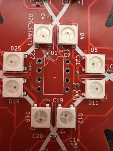
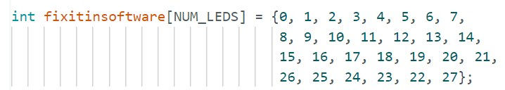
When I turn on the board for the first time, I realize I messed up the LED routing too. Five LEDs are placed out of order, which would disrupt the flow of the flower pattern. My first instinct is to dig up and rewire two traces per misplaced LED, for a total of 50 traces across all of the boards, but there’s a much faster solution here.
Unlike the microcontroller pin mishap, this one can be fixed with code! The ATtiny microcontroller is basically a more lightweight Arduino and can be programmed in a very similar way.
This array tells us the order that each LED is “actually” supposed to be in. Basically, what the microcontroller sees as LED #26 should actually be the 21st to light up.
based on my limited knowledge of electrical engineering, it’s kind of a joke to “fix [hardware problems] in software” because it’s often a bandaid solution to a bigger problem.
once again fixing things in software!
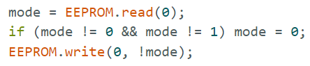
The ATtiny is able to store 512 bytes of EEPROM, which is memory that doesn’t get erased when it’s turned off. Here, the first byte of EEPROM stores the last pattern that was displayed. When the board is turned on again, it simply displays the other pattern.
Sometimes it’s not your fault, but you gotta fix it anyways
The lights flash in the right order. The flower flows. I’m done!
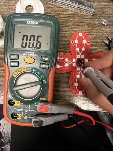
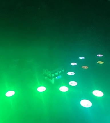
…until I notice that some of the LEDs are acting kind of weird. At least one or two LEDs from each of the five boards aren’t displaying the right color. Poking around with an oscilloscope confirms that my microcontroller is sending the right signals. I dealt with the signal timings for this kind of LED extensively for my 6.115 final project, so I’m pretty confident that I’m not the one at fault here.
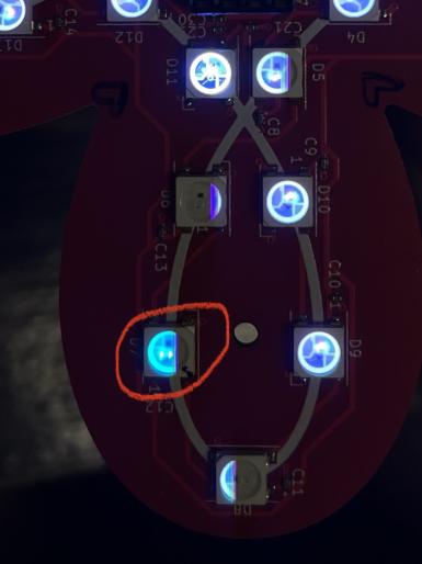
it’s kind of hard to tell here because the camera’s frame rate isn’t lined up with the LED update rate, but the circled LED’s red component is broken :(
The PCB manufacturer must have given me faulty LEDs. Aaaaaaaaaa
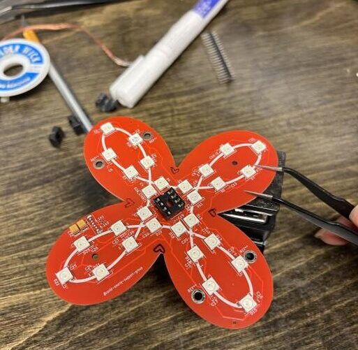
Winnie shows me two ways to replace the faulty LEDs. One way is to use a hot plate and melt the solder joint holding the LED to the board into a puddle of quicksilver. Using tweezers, replace the faulty LED with a new one. Then add a drop of flux to facilitate the new electrical connection and watch the feathery wisps of flux smoke dissipate into the air like ghostly birds.
The other way involves taking a soldering iron and literally melting off the LED. The more burnt plastic particles you release into the atmosphere, the better.03 /s It’s quick and literally dirty.
Because I’m not a big fan of inhaling carcinogens, I eventually get the hot plate method to work even for the inconveniently located LEDs. If I place the board on the hot plate for long enough, the heat eventually reaches said inconvenient location to release the faulty LED. I just have to be careful to not accidentally knock off the nearby non-faulty components. The hot plate doesn’t discriminate: it melts all of the solder joints in its vicinity whether or not you want it to.
If I don’t heat up the solder joints long enough before trying to tweeze out the faulty LEDs, I delaminate the trace. Fortunately, a bit of tape and more caution with resoldering the replacement LED goes a long way.
noooo
Finishing touches
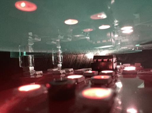
Diffusing the light with a lasercut piece of acrylic scatters and softens the LEDs:
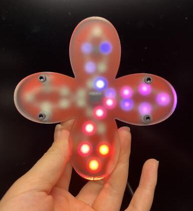
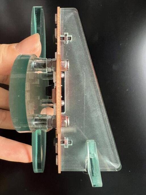
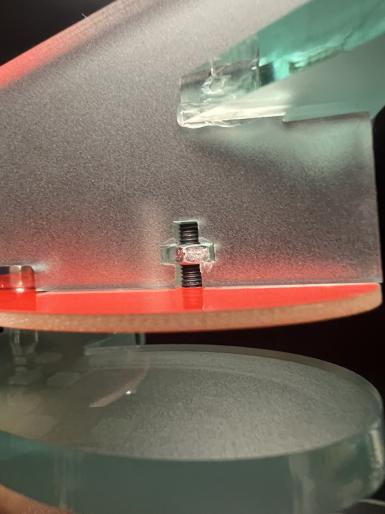
A flower that lights up is cool, but a flower that lights up and stands on its own is even cooler. I lasercut another piece of acrylic to make a screw on stand.
TADA!!!!!!!!

fire mode!!
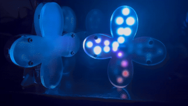
part of rainbow mode! unfortunately including the full rainbow cycle would make the gif too large to upload here
There’s something meditatively calming to watching the lights cycle through the petals, around and around and around. It reminds me of the horror manga Uzumaki by Junji Ito, where a cursed town becomes increasingly obsessed with spirals,04 think eddies in a river, the cochlea (spiral shaped part of the inner ear), a mosquito's proboscis, etc until the townspeople and soon the physical town itself literally become one with the spiral. I don’t blame them; spirally patterns really are mesmerizing.
- Electronics for Mechanical Systems II back to text ↑
- lab assistant back to text ↑
- /s back to text ↑
- think eddies in a river, the cochlea (spiral shaped part of the inner ear), a mosquito's proboscis, etc back to text ↑