
[Liveblog] MARC 2025 by Andi Q. '25
A sciencey science conference, feature Anika '26 and me
Day 1, 6 PM
Today is the first day of MARC 2025 (the Microsystems Annual Research Conference) – MIT’s Microsystems Technology Laboratory’s (MTL) annual conference, featuring two days of MIT students presenting their research to MTL’s industry sponsors like Lam Research and GlobalFoundries. It’s also a (heavily subsidized) ski trip! Because MARC isn’t only about serious science; it’s also an opportunity for the MTL community to get together and have fun before the spring semester starts.
Unlike last year, when I tagged along at MARC despite my nonexistent research output (I guess being an undergrad made it okay), I have a poster to present this year! (Stay tuned until day 2 to see it.) Also unlike last year, when our blogs were restricted to use only the top 1000 most common English words, I can describe things in a non-caveman-like way this year! Goodbye “sticking-together rocks”; hello “magnets”!
Anika ’26 is here too, which was a pleasant surprise!
I look dead inside here, but I assure you I was very excited for the conference. It was just that I had to wake up at 6 AM.
The conference kicked off at 10 AM with “winter activities” at the ski resort by our hotel. I went snowboarding, while Anika went cross-country skiing. It was my first time ever snowboarding; I went skiing last year during MARC and thought the snowboarding people looked so cool, so I decided to give it a shot this year.
Unfortunately, I severely underestimated the difficulty of snowboarding, which I quickly realized as I fell onto my face within the first ten seconds of going down the bunny slope. It turns out that snowboarding is completely different from skiing, skateboarding, or any other sport I’ve tried before. It’s fast, terrifying, and cold. (Just like MIT.) But it was really fun and I loved it, even though my body now hurts everywhere because I kept falling on my face. (Just like MIT.)


I heard Anika had a great time cross-country skiing though, with none of the wipeouts I endured during snowboarding.
Anyway, after all that excitement, we got to the hotel and checked in. I’m currently sitting in the lobby writing this post while I wait for the opening ceremony (and dinner!) to begin. Be back in ~1 hour.
Day 1, 9 PM
Ok, so that was much longer than 1 hour, but the opening banquet had a lot going on and it felt wrong to pull out my laptop (under my seat) and blog during dinner. But now it’s time for the conference’s evening activities, so I finally have a chance to update you on what happened.
The banquet started with Professor Tomas Palacios (director of MTL) giving a presentation with opening remarks. Apparently, MARC has over 300 people attending this year! Anyway, Professor Palacios has a very… unique style of presentation that is best experienced visually. (Apologies in advance for the jank pictures.)
Part 1:


Part 2:


Part 3:


Next, there was an MTL-themed trivia game. Even though we got ~10 people per team, the questions were still rather tricky. Try to see how many of these you can answer (without Googling)!
-
Name the iPod series that had seven generations between 2005 and 2012, included the first iPod with a video camera, and had iPods with both click wheels and touch screens.
- Name the song by American pop band The Postal Service that features two people wearing cleanroom suits in a microelectronics lab.
- What does “CHIPS” stand for in “CHIPS Act”?
- What is the band gap of intrinsic silicon?
- Which wavelength of light are human eyes most sensitive to?
- Name 5 artists with the word “little” or “lil” in their name.
- Who was the first director of MTL?
- What is the total square footage of MIT.nano?
- What is the shortcut for a backward search in the GNU Nano text editor?
-
In which year was the Northeast Microelectronic Coalition formed?
-
Which MIT president, acting or past, also served as an MITL director?
-
Name the largest coral reef in the world and where it is located.
Nobody at my table knew what “CHIPS” stood for, so we guessed “creating happy international packaged semiconductors”. Somehow, this still sounds more realistic than the real answer.
After dinner, there was an “academia vs. industry” panel, with four MIT professors and three industry representatives from Lam Research, IBM, and GlobalFoundries:
- Q: “From an R&D perspective, how does industry benefit from the relative freedom and higher risk tolerance of academic research?”
- Lam Research: Academic research is cool because it helps them identify potentially disruptive technologies from the earliest stages of development, like soft robotics for equipment maintenance. Also, universities are uniquely set up to synthesize and test a huge range of different chemicals (albeit in small batches), whereas industrial processes are typically optimized for synthesizing a small handful of chemicals.
- IBM: They’re heavily involved in university research (particularly MIT) because “[they] cannot invent everything in industry”. It’s also great for “workforce development” (i.e., recruitment).
- GlobalFoundries: What Lam Research and IBM said.
- Q: “How can universities structure their labs to align with industry needs while still adhering to the fundamental goal of original academic research?”
- Professor Jelena Notaros: Having access to industry know-how and tools often just means that research becomes more efficient. Also, original academic research still happens organically because the fresh minds of grad students naturally come up with new ideas that industry veterans may overlook.
- Professor Song Han: Having access to free GPUs is super helpful for AI research, and the industry needs are typically what the grad students want to research anyway. Having industry connections also helps expose students to real-world problems through internships, which can better inform their future research.
- Professor Duane Boning: It’s also often good not to align completely with industry needs, as orthogonal research directions from industry needs is often how the most disruptive new technologies get created.
- Q: “In your respective sectors, how does the pressure for immediate commercial outcomes influence your research, and does the pressure steer you away from fundamental research toward applied research? How do you balance it?”
- GlobalFoundries and IBM: (Idk I wasn’t paying attention to them, but their answers didn’t answer the question anyway.)
- Lam Research: It’s important to communicate the scope and time frame of projects with academic collaborators. Professors typically want funding for at least one year, which limits how short-term/immediate the research can be. Longer-term roadmaps allow for more fundamental research, and that’s often also what companies want anyway without realizing it.
- Professor Song Han: “We use short-term projects to generate cash flow for our long-term projects.”
(I stopped paying attention at this point because it was getting late and I was still physically exhausted from snowboarding earlier today. I think they just talked about the importance of recruitment until the end of the panel.)
It’s probably time for me to go to sleep now, so I’ll see you all tomorrow at 9 AM when the conference switches gear into academic mode.
Day 1, 9:45 PM
Oh actually, one more thing before I go – one of my friends mentioned that the hotel looks a lot like the Overlook Hotel from The Shining, and now I can’t unsee it.

Day 2, 7:30 AM
1.5 hours before the conference begins! Until then, check out this year’s entries for the MTL photo competition:


I think #15 (“Hitting the slopes at MARC”) looks the coolest, but #2 (“SEM photo of unknown particle on plastic substrate which is ruining my device ☹“) best captures the essence of microelectronics research.
Day 2, 9:30 AM
We started off the day with some opening remarks from Professor Vladimir Bulovic, director of MIT.nano. His talk was all about how it takes “just moments” to think of groundbreaking inventions, but several years (sometimes decades) to scale up those inventions to have a tangible impact on the world. Some examples he gave:
- Strained silicon: A processing technology that improves the charge carrier transport properties of silicon. Invented in 1990, but only became widely used in 2003 by Intel in chip manufacturing.
- High-κ dielectrics: Materials that can become more “polarizable” under an electric field, which allows for even smaller transistors. First measured in 1993, but only became used by IBM to create transistors in 2007.
- FinFETs: A transistor structure that uses 3D structure to improve performance. First patented in the 1980s, but only became widely used in 2011 by Intel in chip manufacturing. (Fun fact: FinFETs rely on the two innovations I mentioned above, so this is like innovation squared.)
It’s a bit depressing to think about how long it takes for academic research to become “useful”, but that’s exactly what MIT.nano and initiatives like the CHIPS and Science Act are trying to change.
Another cool thing Professor Bulovic talked about was all the big players of the semiconductor industry that were MIT alumni:
- Cecil Green (MS 1924): Founder of Texas Instruments.
- William Shockley (PhD 1936): Co-inventor of the transistor.
- Morris Chang (MEng 1955): Founder of TSMC.
- Ray Stata (SM 1958; pronounced “stay-ta” not “stah-ta”): Founder of Analog Devices.
- Irwin Jacobs (PhD 1959): Founder of Qualcomm.
- Robert Metcalfe (BS 1969): Inventor of ethernet and much of the early internet.
- Robert Noyce (PhD 1953): Founder of Fairchild Semiconductor and Intel.
Day 2, 10:30 AM
We have a 20-minute break before the poster sessions and 1-minute poster pitches (the most exciting non-ski part of the conference). Right before this, we had a keynote talk from Deirdre Hanford, CEO of Natcast. Natcast isn’t really a commercial company like IBM or Lam Research, but more a non-profit consortium that generally works to advance the US semiconductor industry.
The talk was mostly about the National Semiconductor Technology Center’s (NSTC) goals, like “extend US semiconductor leadership” and “reduce time and cost to prototype” – a lot of which was already discussed in earlier talks at MARC.
The talk also focused on the skyrocketing energy consumption of AI. For example, did you know that Google’s LLM-powered search results use more than 25x more energy than a traditional Google search? That Sam Altman wants to create an OpenAI datacenter that will consume as much power as Miami? And that datacenters in Virginia consume about a quarter of the state’s power? Once again, AI is the worst.
Day 2, 11 AM
Pitch time! Here are some people’s projects (most people opted not to do a pitch), in rapid-fire:
- Session 1: Quantum Science and Engineering
- S2.04: “Quantum-secure deep learning”: A physical data transfer protocol designed to leak minimal data, e.g. so that healthcare AIs don’t leak information to insurance companies.
- S2.07: “Electron energy loss spectroscopy of 2D materials in an SEM”: A more effective way to image 2D materials using electrons and quantum effects.
- S2.10: (Honestly not sure what this one is about, but the pitch was quite entertaining. “If you want to understand, you should come to [my poster]”.)
- S2.16: “Integrated photonics for polarization-gradient cooling of trapped ions”: A way to shrink quantum computers from taking up an entire room to fit on a chip the size of your fingertip.
- Session 5: Electronic, Magnetic, and Spintronic Devices
- S5.13: “Hafnium-zirconium-oxide ferroelectric materials for advanced logic and memory technologies”: An exotic new material with negative capacitance for more efficient computing.
- S5.26: “High-performance multi-channel MoS2 transistors for front-end-of-line integration beyond 1 nm node”: Ultra tiny, 2D transistors.
- Session 6: Medical Devices and Biotechnology
- S6.01: “New NMR probe configurations for spectroscopy and relaxometry of moving fluids”: A new process for doing NMR scans on moving samples, allowing for easier integration with industrial processes.
- S6.15: “Deep and dynamic metabolic and structural imaging of living tissues”: A way to peek deep into living tissue using infrared light, without needing to cut into the tissue.
- Session 9: Neuromorphic Devices and AI Hardware Accelerators
- S9.01: Some kind of simulator for AI hardware accelerators I think.
- S9.03: “Analog accelerators for modern Hopfield networks”: Another hardware AI accelerator.
- S9.11: “SORBET: secure off-chip memory interface for deep neural network accelerators”: A secure computer memory architecture for AI accelerators
- S9.13: “SVDQuant: absorbing outliers by low-rank components for 4-bit diffusion models”: I’m sure there’s serious science here but the guy burst into song halfway through the pitch and I completely forgot what the rest of it was about.
- S9.18: “Tailor Swiftiles: accelerating sparse tensor algebra by overbooking buffer capacity”: Treating computer memory like a concert hall and “overbooking seats” to improve its efficiency.
- S9.20: “Quantum-noise-limited optical neural networks using a few quanta per neuron activation”: A neural network that can recognize digits using light.
- Session 10: Circuits and Systems
- S8.10: “Continuous bladder monitoring”: A wearable ultrasound medical device with extremely high power efficiency.
Day 2, 1 PM
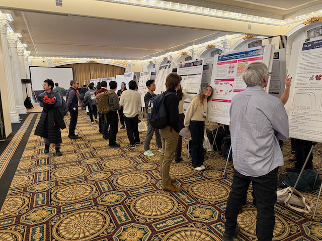
After the 1-minute pitch session, we had our first poster session of the day.
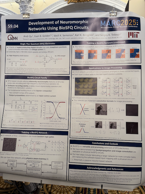
Here’s my poster:
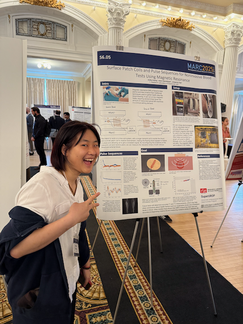
And Anika’s!
I wish I could’ve walked around more to see what everyone else’s posters were about, but I had to stand near my poster and answer questions about it. Some of the questions people asked I didn’t know how to answer completely (e.g. “how do Josephson junctions work?”), which was a little scary, but they seemed okay with that.
Day 2, 1:30 PM
On a somewhat unrelated note, Professor Karl Berggren (the professor I do research with) is officially the new head of electrical engineering at MIT!
Day 2, 2:30 PM
I’m currently at a panel about transitioning from academia to startups. The panelists include two MTL-affiliated startup founders (the companies are FabuBlox and Active Surfaces), a founding partner of a venture capital firm, and Professor Dave Perrault (also a startup founder and head of house for Simmons). FabuBlox makes software for designing nanofabrication processes, while Active Surfaces makes printable solar panels that can stick onto any surface.
I’m not very entrepreneurial at all, but it was still interesting to hear from this panel because hardware and “deep tech” startups are much rarer than (and completely different from) software and AI startups that I’m more familiar with. The advice they gave was also very reasonable (none of that “drop out of MIT” that software startup bros tend to spew out):
- Take advantage of MIT’s patenting office (apparently this is a thing and they help you monetize your inventions) and other startup incubation resources. MIT really loves being affiliated with successful startups, so they will throw a lot of money at you to help you succeed.
- Do a lot of market research and think deeply about whether your idea is actually worth turning into a startup before dropping everything and starting a company.
- Don’t go around telling people about how your innovative new technology works, even if it is protected by patents. (This is the opposite of academia, where sharing knowledge in as much detail as possible is the norm.)
- Don’t do illegal things.
Day 2, 3 PM
Round 2 of poster pitches! (I forgot to link this previously, but you can match these descriptions to their official titles here.)
- Session 1: Materials Synthesis and Characterization
- S1.01: Semiconducting polymers that can detect neurotransmitters like dopamine. These polymers can help treat mental disorders caused by chemical imbalances in the brain.
- S1.02: A neural network that can precisely measure tiny angle differences between two overlapping 2D materials.
- S1.07: A robot that synthesizes graphene 24/7. (Graphene is actually quite hard to synthesize so I’m surprised that a robot can do this.)
- S1.08: A technique for synthesizing graphene with holes of controllable sizes.
- Session 3: Photonics and Optoelectronics
- S3.06: A robot that can design and build optical communication systems.
- S3.09: A tiny chip that can sense hydrogen gas.
- S3.14: Augmented reality glasses without the bulky supporting electronics.
- S3.16: Better LiDAR sensors for autonomous vehicles.
- S3.18: Same as the above but different somehow.
- S3.19 and S3.22: Some kind of optics/laser physics magic that I don’t understand.
- S3.23: Tiny antennas made of gold that can detect infrared radiation much better than existing sensors.
- Session 4: Power Devices and Circuits
- S4.02: More efficient electric motors somehow (I don’t understand power electronics oops).
- S4.06: Using aluminum nitride (typically used as an insulator) as a semiconductor to make efficient power transistors.
- S4.08: Piezoelectricity-based energy conversion.
- Session 7: Nanoscience and Nanotechnology
- S7.22: Graphene supercapacitors for energy storage.
- Session 10: 3DHI and Additive Manufacturing
- S10.04: 3D-printed magnets with any shape you want.
- Session 11: MEMS, Field Emitter, Thermal, and Fluidic Devices and Robotics
- S11.02: Some kind of neural network training algorithm. (Not sure why it’s in this section and not the general AI section though.)
- S11.07: Insect-sized robots that can jump and fly.
- S11.08: More memory-efficient robot vision (I think).
Day 2, 5 PM
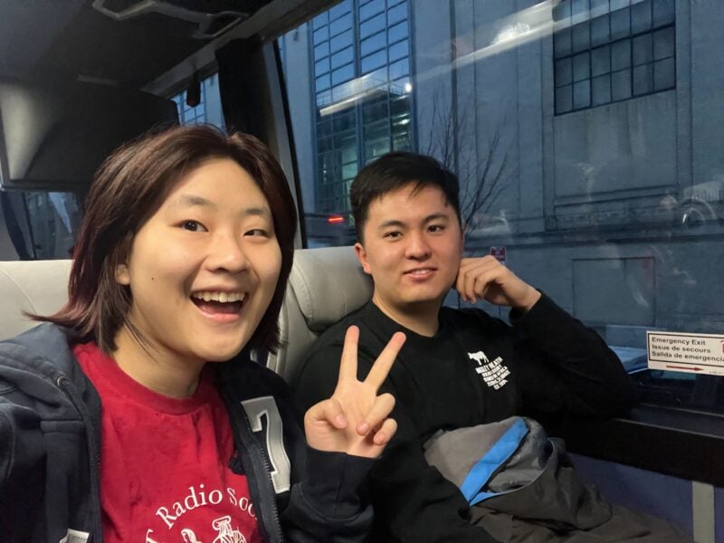
A second poster session and some closing remarks later, and MARC 2025 is over! What a fun conference this has been. Anika and I are on the bus back to MIT now, but the adventure isn’t quite over yet – stay tuned for Anika’s version of events, coming to an MIT Admissions near you.